- 您现在的位置:买卖IC网 > Sheet目录1998 > ICS844201BG-45LF (IDT, Integrated Device Technology Inc)IC CLK GENERATOR 25MHZ 8TSSOP
ICS844201I-45 Data Sheet
FEMTOCLOCK CRYSTAL-TO-LVDS CLOCK GENERATOR
ICS844201BKI-45 REVISION A OCTOBER 7, 2013
4
2013 Integrated Device Technology, Inc.
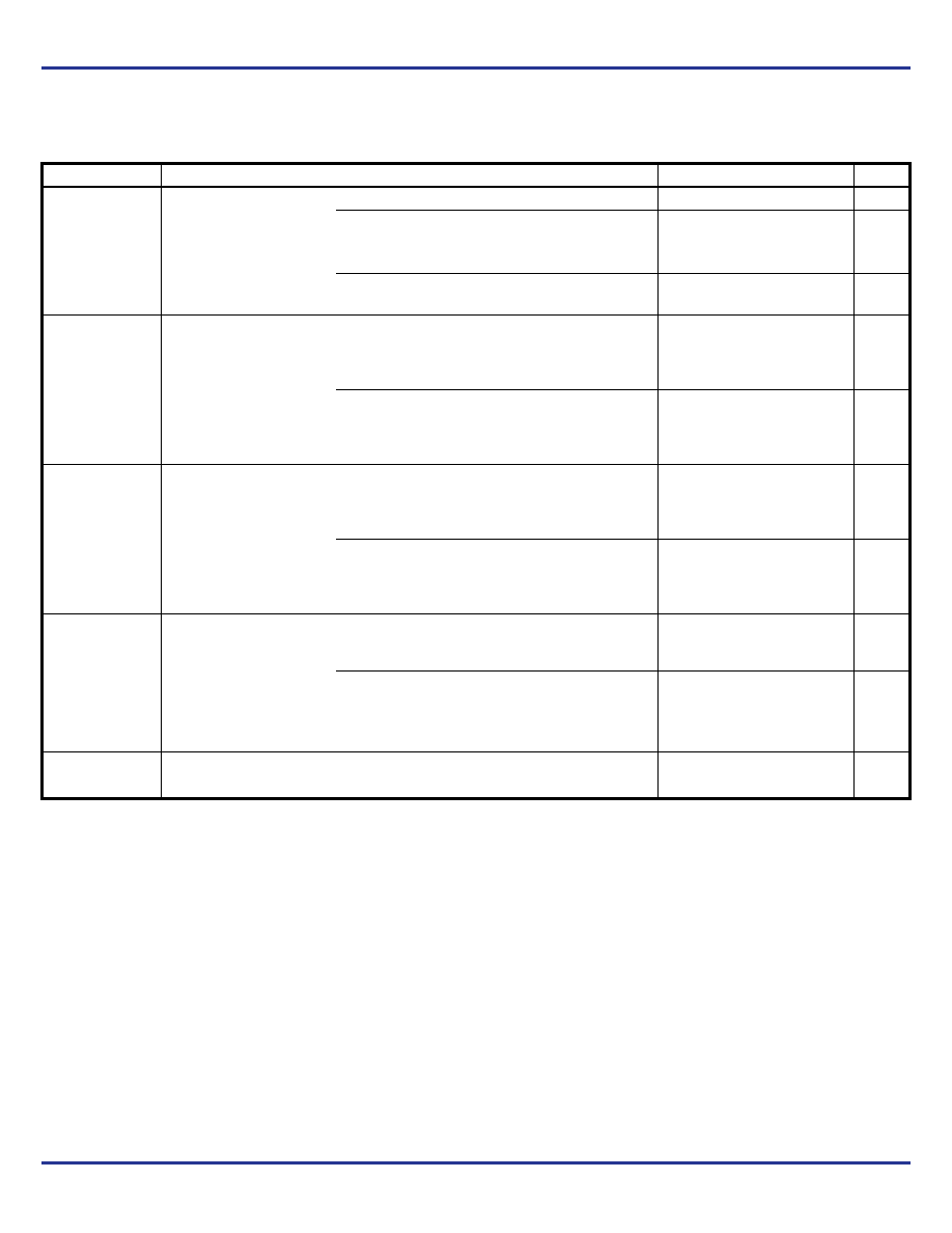
AC Electrical Characteristics
Table 5. AC Characteristics, VDD = 3.3V ± 10%, TA = -40°C to 85°C
NOTE: Electrical parameters are guaranteed over the specified ambient operating temperature range, which is established when the device is
mounted in a test socket with maintained transverse airflow greater than 500 lfpm. The device will meet specifications after thermal equilibrium
has been reached under these conditions.
NOTE: Characterized using a 25MHz crystal.
NOTE 1: Refer to Phase Noise Plots.
NOTE 2: Peak-to-Peak jitter after applying system transfer function for the Common Clock Architecture. Maximum limit for PCI Express Gen 1
is 86ps peak-to-peak for a sample size of 106 clock periods. See IDT Application Note PCI Express Reference Clock Requirements and also
the PCI Express Application section of this datasheet which show each individual transfer function and the overall composite transfer function.
NOTE 3: RMS jitter after applying the two evaluation bands to the two transfer functions defined in the Common Clock Architecture and
reporting the worst case results for each evaluation band. Maximum limit for PCI Express Generation 2 is 3.1ps rms for tREFCLK_HF_RMS
(High Band) and 3.0 ps RMS for tREFCLK_LF_RMS (Low Band). See IDT Application Note PCI Express Reference Clock Requirements and also
the PCI Express Application section of this datasheet which show each individual transfer function and the overall composite transfer function.
Symbol
Parameter
Test Conditions
Minimum
Typical
Maximum
Units
fOUT
Output Frequency
125
MHz
100
MHz
tjit()
RMS Phase Jitter,
Random; NOTE 1
125MHz, Integration Range:
12kHz – 20MHz
0.773
ps
100MHz, Integration Range:
12kHz – 20MHz
0.792
ps
tj
Phase Jitter
Peak-to-Peak;
NOTE 2
125MHz, (1.2MHz – 21.9MHz)
25MHz crystal input
Evaluation Band: 0Hz - Nyquist
(clock frequency/2)
12.51
ps
100MHz, (1.2MHz – 21.9MHz)
25MHz crystal input
Evaluation Band: 0Hz - Nyquist
(clock frequency/2)
13.48
ps
tREFCLK_HF_RMS
Phase Jitter RMS;
NOTE 3
125MHz, (1.2MHz – 21.9MHz)
25MHz crystal input
High Band: 1.5MHz - Nyquist
(clock frequency/2)
1.13
ps
100MHz, (1.2MHz – 21.9MHz)
25MHz crystal input
High Band: 1.5MHz - Nyquist
(clock frequency/2)
1.25
ps
tREFCLK_LF_RMS
Phase Jitter RMS;
NOTE 3
125MHz, (1.2MHz – 21.9MHz)
25MHz crystal input
Low Band: 10kHz - 1.5MHz
0.32
ps
100MHz, (1.2MHz – 21.9MHz)
25MHz crystal input
Low Band: 10kHz - 1.5MHz
0.33
ps
tR / tF
Output Rise/Fall Time
20% to 80%
250
450
ps
odc
Output Duty Cycle
fOUT = 125MHz
48
52
%
fOUT = 100MHz
46
54
%
发布紧急采购,3分钟左右您将得到回复。
相关PDF资料
ICS844204BK-245LF
IC CLK SYNTHESIZER 4LVDS 32VFQFN
ICS844S42BKILF
IC SYNTHESIZER RF FREQ 56-VFQFPN
ICS86004BG-01LF
IC CLK BUFFER ZD 1:4 16-TSSOP
ICS8634BY-01LFT
IC BUFFER ZD 1-5 LVPECL 32-LQFP
ICS8701AY-01LF
IC CLK GEN POLARITY CTRL 48-LQFP
ICS8701CYLF
IC CLK GENERATOR /1 /2 48-LQFP
ICS870931ARI-01LF
IC CLK GENERATOR LVCMOS 20QSOP
ICS87158AFLF
IC CLOCK GEN 1-6 HCSL 48-SSOP
相关代理商/技术参数
ICS844201BG-45LFT
功能描述:IC CLK GENERATOR 25MHZ 8TSSOP RoHS:是 类别:集成电路 (IC) >> 时钟/计时 - 专用 系列:HiPerClockS™, FemtoClock™, PCI Express® (PCIe) 标准包装:1,500 系列:- 类型:时钟缓冲器/驱动器 PLL:是 主要目的:- 输入:- 输出:- 电路数:- 比率 - 输入:输出:- 差分 - 输入:输出:- 频率 - 最大:- 电源电压:3.3V 工作温度:0°C ~ 70°C 安装类型:表面贴装 封装/外壳:28-SSOP(0.209",5.30mm 宽) 供应商设备封装:28-SSOP 包装:带卷 (TR) 其它名称:93786AFT
ICS844201BGI-45LF
功能描述:IC CLK GENERATOR 25MHZ 8TSSOP RoHS:是 类别:集成电路 (IC) >> 时钟/计时 - 专用 系列:HiPerClockS™, FemtoClock™, PCI Express® (PCIe) 标准包装:1,500 系列:- 类型:时钟缓冲器/驱动器 PLL:是 主要目的:- 输入:- 输出:- 电路数:- 比率 - 输入:输出:- 差分 - 输入:输出:- 频率 - 最大:- 电源电压:3.3V 工作温度:0°C ~ 70°C 安装类型:表面贴装 封装/外壳:28-SSOP(0.209",5.30mm 宽) 供应商设备封装:28-SSOP 包装:带卷 (TR) 其它名称:93786AFT
ICS844201BGI-45LFT
功能描述:IC CLK GENERATOR 25MHZ 8TSSOP RoHS:是 类别:集成电路 (IC) >> 时钟/计时 - 专用 系列:HiPerClockS™, FemtoClock™, PCI Express® (PCIe) 标准包装:1,500 系列:- 类型:时钟缓冲器/驱动器 PLL:是 主要目的:- 输入:- 输出:- 电路数:- 比率 - 输入:输出:- 差分 - 输入:输出:- 频率 - 最大:- 电源电压:3.3V 工作温度:0°C ~ 70°C 安装类型:表面贴装 封装/外壳:28-SSOP(0.209",5.30mm 宽) 供应商设备封装:28-SSOP 包装:带卷 (TR) 其它名称:93786AFT
ICS844202AK-245LF
功能描述:IC CLOCK GEN SRL SCSI 32-VFQFPN RoHS:是 类别:集成电路 (IC) >> 时钟/计时 - 专用 系列:HiPerClockS™, PCI Express® (PCIe) 标准包装:28 系列:- 类型:时钟/频率发生器 PLL:是 主要目的:Intel CPU 服务器 输入:时钟 输出:LVCMOS 电路数:1 比率 - 输入:输出:3:22 差分 - 输入:输出:无/是 频率 - 最大:400MHz 电源电压:3.135 V ~ 3.465 V 工作温度:0°C ~ 85°C 安装类型:表面贴装 封装/外壳:64-TFSOP (0.240",6.10mm 宽) 供应商设备封装:64-TSSOP 包装:管件
ICS844202AK-245LFT
功能描述:IC CLOCK GEN SRL SCSI 32-VFQFPN RoHS:是 类别:集成电路 (IC) >> 时钟/计时 - 专用 系列:HiPerClockS™, PCI Express® (PCIe) 标准包装:28 系列:- 类型:时钟/频率发生器 PLL:是 主要目的:Intel CPU 服务器 输入:时钟 输出:LVCMOS 电路数:1 比率 - 输入:输出:3:22 差分 - 输入:输出:无/是 频率 - 最大:400MHz 电源电压:3.135 V ~ 3.465 V 工作温度:0°C ~ 85°C 安装类型:表面贴装 封装/外壳:64-TFSOP (0.240",6.10mm 宽) 供应商设备封装:64-TSSOP 包装:管件
ICS844202AKI-245LF
功能描述:IC CLOCK GEN SRL SCSI 32-VFQFPN RoHS:是 类别:集成电路 (IC) >> 时钟/计时 - 专用 系列:HiPerClockS™, PCI Express® (PCIe) 标准包装:1,500 系列:- 类型:时钟缓冲器/驱动器 PLL:是 主要目的:- 输入:- 输出:- 电路数:- 比率 - 输入:输出:- 差分 - 输入:输出:- 频率 - 最大:- 电源电压:3.3V 工作温度:0°C ~ 70°C 安装类型:表面贴装 封装/外壳:28-SSOP(0.209",5.30mm 宽) 供应商设备封装:28-SSOP 包装:带卷 (TR) 其它名称:93786AFT
ICS844202AKI-245LFT
功能描述:IC CLOCK GEN SRL SCSI 32-VFQFPN RoHS:是 类别:集成电路 (IC) >> 时钟/计时 - 专用 系列:HiPerClockS™, PCI Express® (PCIe) 标准包装:28 系列:- 类型:时钟/频率发生器 PLL:是 主要目的:Intel CPU 服务器 输入:时钟 输出:LVCMOS 电路数:1 比率 - 输入:输出:3:22 差分 - 输入:输出:无/是 频率 - 最大:400MHz 电源电压:3.135 V ~ 3.465 V 工作温度:0°C ~ 85°C 安装类型:表面贴装 封装/外壳:64-TFSOP (0.240",6.10mm 宽) 供应商设备封装:64-TSSOP 包装:管件
ICS844204AK-245LF
功能描述:IC CLK SYNTHESIZR 4OUT 32-VFQFPN RoHS:是 类别:集成电路 (IC) >> 时钟/计时 - 时钟发生器,PLL,频率合成器 系列:HiPerClockS™ 标准包装:1,000 系列:- 类型:时钟/频率合成器,扇出分配 PLL:- 输入:- 输出:- 电路数:- 比率 - 输入:输出:- 差分 - 输入:输出:- 频率 - 最大:- 除法器/乘法器:- 电源电压:- 工作温度:- 安装类型:表面贴装 封装/外壳:56-VFQFN 裸露焊盘 供应商设备封装:56-VFQFP-EP(8x8) 包装:带卷 (TR) 其它名称:844S012AKI-01LFT